
Todays an audio brand name SUNBUCK are starting to fame in my country and now i try to make tracing schematic diagram SUNBUCK AV-80, a cheap audio amplifier with many featured in the unit.
SUNBUCK AV-80 present with USB and Bluetooth communication that is make you sing all day with your favourite song came from USB stick and you sing with your loving microphone.
Table of Contents
INFO
Some reviewers in youtube or another e-commerce said that tha amplifier are 2000W. But I don’t trust they said.
Video looking inside of the Amplifier unit are just not big enough for Power Transformer. This looks like a 200 Watts transformer.
The unit are using Final Power Transistor 2SC5198 in quasi mode and the maximum output are reaching 100 Watt each channel.
It mean that the total Power Output are 200 Watts.
Some feture:
Extra SHDC slot for you to play your song from memory card.
USB port can easily you to play your various karaoke song or others multimedia files.
2 sockets Microphone inlet to make you sing along with your partner.
TRACED SCHEMATIC DIAGRAM SUNBUCK AV-80
Here are the results of traced schematic diagram SUNBUCK AV-80 :

From the circuit above are consist of circuit blocks:
- Differential Preamplifier,
- Voltage Amplifier Stages,
- Driver Amplifier, and finally
- Final Power Amplifier.
All transistors are using cheap transistor 2N5551 and 2N5401 but using Final Power transistors 2SC5198.
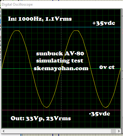
SIMULATING CIRCUIT
The tracing schematic i made is has ready to simulate with software, say it Proteus. This is I always do practice to test the result of my electrical schematic drawing.
The result of simulaton are just like this:
SEE ALSO
Another Audio Power Amplifier inside this blog LOOK HERE.
Blogspot of YOHAN AUDIO LINK HERE.
Supported Video youtube: WARUNG MBAK LINDA