MAGNAT CLASSIC 4000XL is an audio car amplifier made by MAGNAT of 90’s. Its deliver 4 x100 Watts or working in Four Channels amplifier or Two Channels Bridge Tied Load.
OCL 100 Watts LANEY here is a LANEY 100SC made of 90s.
This guitar audio amplifier comes with a 100 Watt audio output with 2 channels. The first channel is for High GAIN Channel, and another one is for CLEAN Channel.
High Gain channel is usually for guitar amps that tend to loud music like ROCK and Metal and other hard genres. CLEAN channel can be used to amplify the sound of guitar genre such as Blues, Country, Ballads, Jazz and other melodics style.
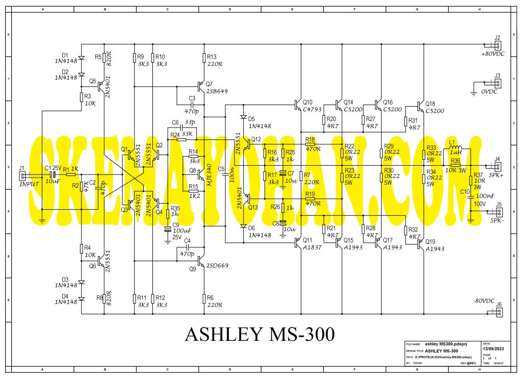
Thanks for vlogger and youtuber that make me translate schematic diagram ASHLEY MS 300.
ASHLEY is an audio Power Amplifier made in Indonesian and has a place in the hearts of his fans. This time I’ll to show you the tracing schematic of AHLEY Power Amplifier MS-300 series.
Table of Contents
INFO
Manufacturer of this Amply saying in their brochure that the SCHEMATIC DIAGRAM ASHLEY MS 300 is stereo 450Wx2 or 900 Watts totals output.
I think this is fair because it’s using 3 pair of C5200/A1943 transistor that came with 150 Watts on each (DATASHEETS).
Where is to purchase the Amplfieir? How price of this Amps?
The list below are many of olshop that sale this amplifier.
In this article I only translate in the Power Amplifier section to make it easier for readers to learn this Power Amplifier.
And here are results of my observations:
Note: This tracing schematic diagram can be wrong in drawing. Don’t hesitate to give me complain and suggestions. Thank you.
Rangkaian ini terdiri dari beberapa blok:
Differential Preamplifier,
Voltage Amplifier Stages,
Servo Driver,
Over Current Protection,
Driver Amplifier, and the last is
Final Power Amplifier.
Actually, there are other features in this SCHEMATIC DIAGRAM ASHLEY MS 300 Power Amplifier that I didn’t mention such as the Speaker Protector feature, Clip Detector, and Under Voltage detector but they I’m not inform it to you.
SEE ALSO
Another schematic diagram in this blog is in THIS LINK.
Hundreds of Edited / Cropped Audio scematic Diagram in Yohan’s Blogspot READ HERE.
Various Built-Up Audio Power and Mixer Schemativ Diagram of YOHAN INDRAWIJAYA.
YOUTUBE VIDEO:
Thanks for many youtube’s videos as writing source below:
Power Ashley Ms300 Wajib Oprek Agar Layak Pake by JD AUDIO
Its interesting to observe a Power Amplifier that below Rp.1M but it can reaching up to 2000 Watts of audio power in SUNBUCK MP326BT. Is it true?
An audio Power Amplifier name SUNBUCK with series number of MP326BT are made from China mainland and it has be sale over the world such as Indonesia, Europe, Russia and others.
In my country, the name are so famous because its a cheap enough to purchased.
FACT OR FAKE: BELOW Rp. 1M but POWER UP TO 2000W
After i saw the video, inside of the Power Amplifier are using a pair of 2S5198 in quasi mode for each channel.
It mean the Power amplifier are 100 Watt maximum output but it only say 60 to 70 Watts in 4 Ohm load.
100W are maximum Power Dissipation of its Final Power transistor and 60/70 are effective output audio power.
This is a inside of the amply and wiring of the power amplifier:
TRACED SCHEMATIC DIAGRAM OF SUNBUCK MP326BT
After a few hours to observe, this is a result of the Power Amplifier section:
Note: Schematic diagram picture above are can be wrong in number of value or wiring.I do tracing the module are with my own perspection.
Block of schematic diagram consist of:
Differential preamplifier,
Voltage Amplifier Stages,
Driver Amplifier, and the last is
Final Power Amplifier.
Power section of SUNBUCK MP326BT are using a quasi power transistor 2Sc5198 that its 100 Watts dissipation output (DATASHEETS).
SEE ALSO
Another Audio Power Amplifier inside this blog LOOK HERE.
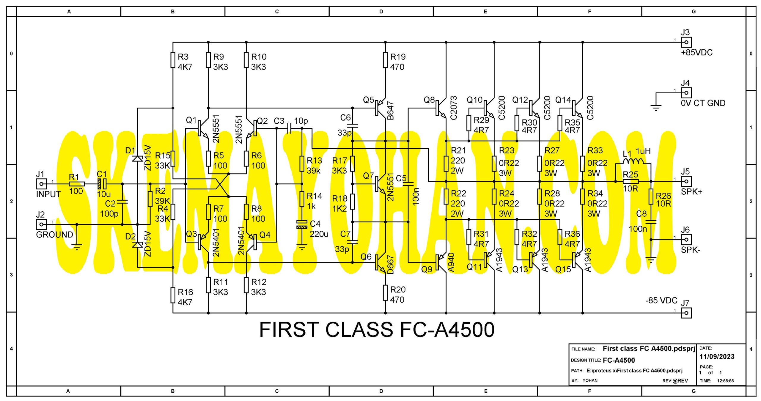
Todays an audio brand name SUNBUCK are starting to fame in my country and now i try to make tracing schematic diagram SUNBUCK AV-80, a cheap audio amplifier with many featured in the unit.
SUNBUCK AV-80 present with USB and Bluetooth communication that is make you sing all day with your favourite song came from USB stick and you sing with your loving microphone.
Table of Contents
INFO
Some reviewers in youtube or another e-commerce said that tha amplifier are 2000W. But I don’t trust they said.
Video looking inside of the Amplifier unit are just not big enough for Power Transformer. This looks like a 200 Watts transformer.
The unit are using Final Power Transistor 2SC5198 in quasi mode and the maximum output are reaching 100 Watt each channel.
It mean that the total Power Output are 200 Watts.
Some feture:
Extra SHDC slot for you to play your song from memory card.
USB port can easily you to play your various karaoke song or others multimedia files.
2 sockets Microphone inlet to make you sing along with your partner.
TRACED SCHEMATIC DIAGRAM SUNBUCK AV-80
Here are the results of traced schematic diagram SUNBUCK AV-80 :
From the circuit above are consist of circuit blocks:
Differential Preamplifier,
Voltage Amplifier Stages,
Driver Amplifier, and finally
Final Power Amplifier.
All transistors are using cheap transistor 2N5551 and 2N5401 but using Final Power transistors 2SC5198.
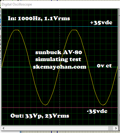
SIMULATING CIRCUIT
The tracing schematic i made is has ready to simulate with software, say it Proteus. This is I always do practice to test the result of my electrical schematic drawing.
The result of simulaton are just like this:
SEE ALSO
Another Audio Power Amplifier inside this blog LOOK HERE.
Tulisan ini adalah tentang modifikasi sebuah power lawas untuk menjadi OCL 600 Watts 80V dengan menggunakan skema dari ampli buatan ROTEL.
Seri yang saya gunakan untuk bahan tulisan ini adalah ROTEL seri RA-921 yang terkenal pada era 90-an.
Table of Contents
Pada saat itu Power ini hanya menggunakan tegangan kerja 28 VDC simetris dan 1 pasang transistor saya dengan dissipasi daya 100 Watts.
Lho kok bisa berubah menjadi 600 Watt? Jawabnya simpel saja. Tegangan dinaikkan, komponen ada yang berubah, ada yang ditambah, dan transistor Final saya perbanyak hingga 6 pasang 2SC5200 / 2SA1943.
Berikut adalah penampakan isi dalam Power Rotel RA921:
x
SKEMA OCL 600 WATTS 80V
Selanjutnya saya mencoba mencari skema power amplifier dari servis manualnya. Ambil DI SINI.
Dan hasil gambar ulang menjadi seperti di bawah ini:
Komponen yang terlibat di sini termasuk sederhana dan umumnya driver amplifier di negeri kita.
Blok rangkaian ini terdiri dari:
Preamp differensial,
Penguat tegangan,
Servo Driver,
Driver 1,
Driver 2
KLONING DRIVER 921
Selanjutnya saya melakukan percobaan untuk melakukan kloning pada rangkaian power amplifier ini dan menghasilkan PCB seperti gambar di bawah ini:
Dari PCB ini nampak bahwa saya menggunakan skun terminal untuk mempermudah join kabel antara kit Driver ini dengan papan Final.
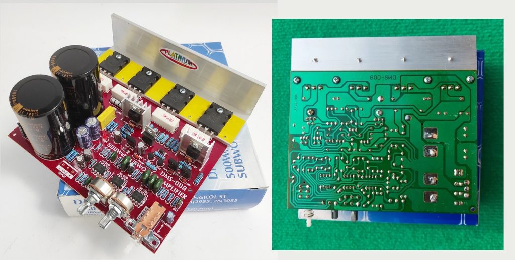
Pada suatu hari saya melihat ada sebuah kit Power amplifier untuk Subwoofer dengan nama 500W SUBWOOFER AMPLIFIER DMS dengan kode kit 009.
Kit buatan PLATINUM ini hampir selalu ada di toko elektro di kota saya dan mungkin ada juga di kota anda.
DMS sepertinya adalah sebuah kode produksi dari sebuah bisnis yang bernama PLATINUM.
Banyak sekali macam-macam kit amplifier dengan seri macam-macam dengan kode depan DMS. Dan DMS009 ini menarik perhatian saya untuk saya teliti.
Table of Contents
PCB DAN KIT SUBWOOFER AMPLIFIER DMS009
Foto ini adalah bahan saya untuk observasi rangkaian Power Subwoofer buatan DMS.
Setelah saya teliti ternyata rangkaian ini adalah Power Mono atau tunggal meskipun inputnya adalah Stereo / Dual.
Dengan melihat jumlah transistor final adlaah 2 pasang maka dapat dipastikan bahwa rangkaian ini memiliki kemampuan daya sampai 300 Watt saja mengingat kemampuan transistor Final adalah hanya sampai 150 Watt (DATASHEETS).
SKEMA HASIL TRACING SUBWOOFER 500W
Berikut ini adalah skema hasil tracing atas kit PCB dan jalurnya yang saya peroleh dari internet:
Note: Pada skema ini banyak sekali komponen dengan nilai “X”, ini berarti bahwa saya tidak menyertakan nilai komponen tersebut karena bahan untuk tracing dan observasi adalah kurang jelas sehingga sulit bagi saya untuk mengetahui nilai komponen tersebut. Kritik dan saran dari anda adalah diperlukan.
Dari terjemahan ini maka kita bisa lihat bahwa SUBWOOFER AMPLIFIER DMS terdiri dari beberapa blok, antara lain:
Penguat sinyal,
Mixer amplifier,
Filter Subwoofer,
Phase Shifter / pembalik fasa,
Preamplifier,
Voltage Amplifier Stages,
Driver Amplifier, dan terakhir adalah
Final Power Amplifier.
Penguat sinyal di sini adalah memperkuat sinyal input kiri dan kanan yang rata-rata 1Vpp untuk naik menjadi beberapa vpp untuk pencampuran.
Mixer amplifier di sini adalah OPAMP U2A bertugas untuk mencampur 2 sinyal dari input kiri dan kanan.
BACAAN LAINNYA
Macam macam skema Power Amplifier dalam Blog ini BACA SINI.
Sebuah skema menarik perhatian saya yang saya temukan di medsos di situ mengatakan bahwa layout PCB bernama DRIVER 132CC oleh seorang kreator PCB desainer yang bernama Joe Sahara dari Indonesia.
Di negeri ini, banyak sekali para lay-outer PCB dan desainer rangkaian audio berbagai kelas / topologi.
Desain PCB ini saya peroleh dari medsos dan menarik untuk review. Melihat PCB silahkan LIHAT SINI.
Table of Contents
SKEMA TRACING DRIVER 132CC
Berikut adalah skema hasil tracing atas PCB driver 132CC ini:
Note: skema ini bisa saja salah dalam penempatan komponen maupun wiring karena saya hanya berpatokan pada gambar PCB yang tengah saya observasi. Kritik dan saran sangat diperlukan.
Dari skema ini nampak bahwa rangkaian terdiri dari blok:
Preamplifier differensial,
Penguat Tegangan,
Servo Driver,
Driver Amplifier 1, dan terakhir
Driver Amplifier 2.
Skea DRIVER 132CC ini telah berhasil saya simulasi dan hasilnya adalah respon frekwensinya bagus.


