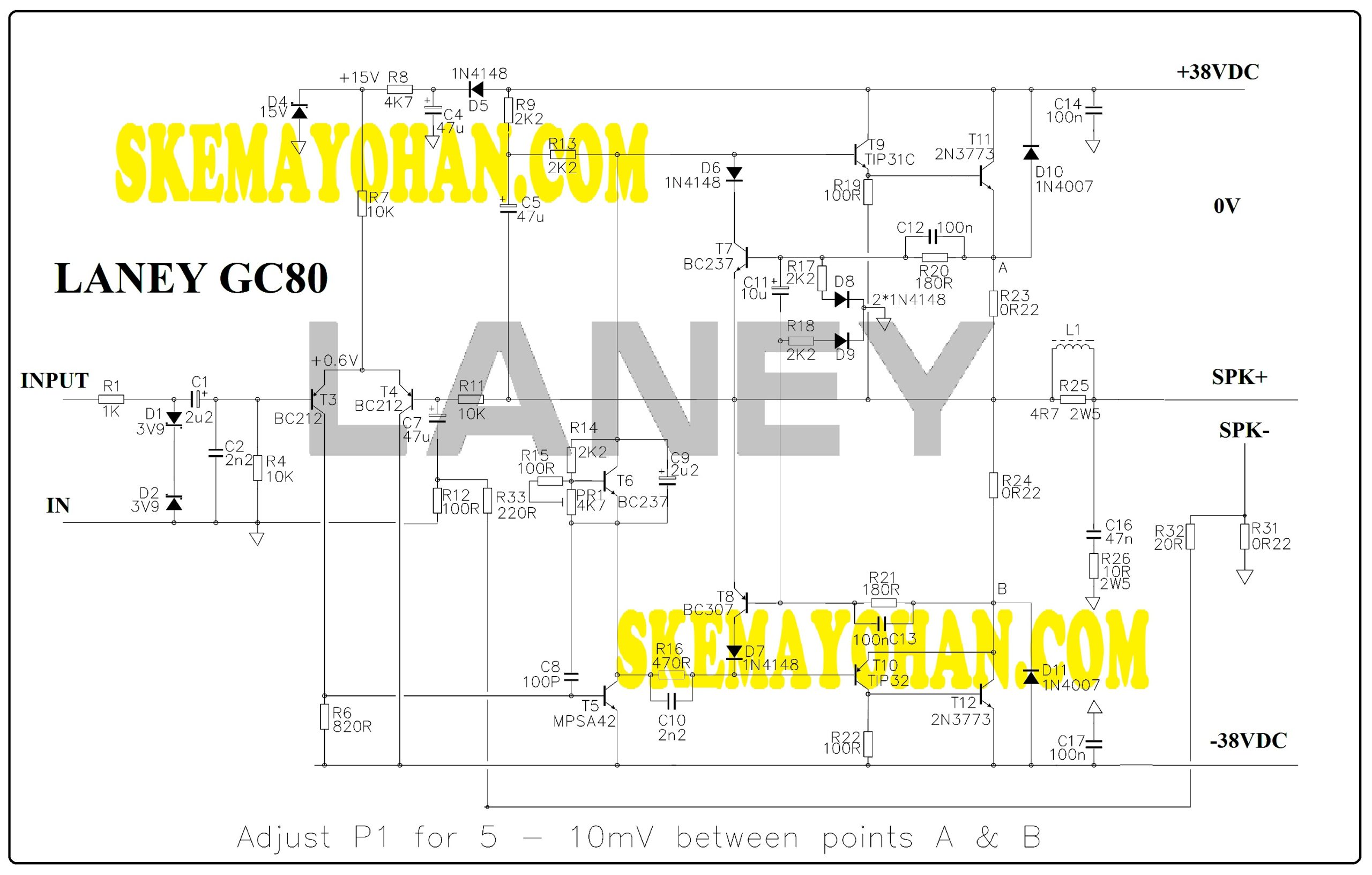
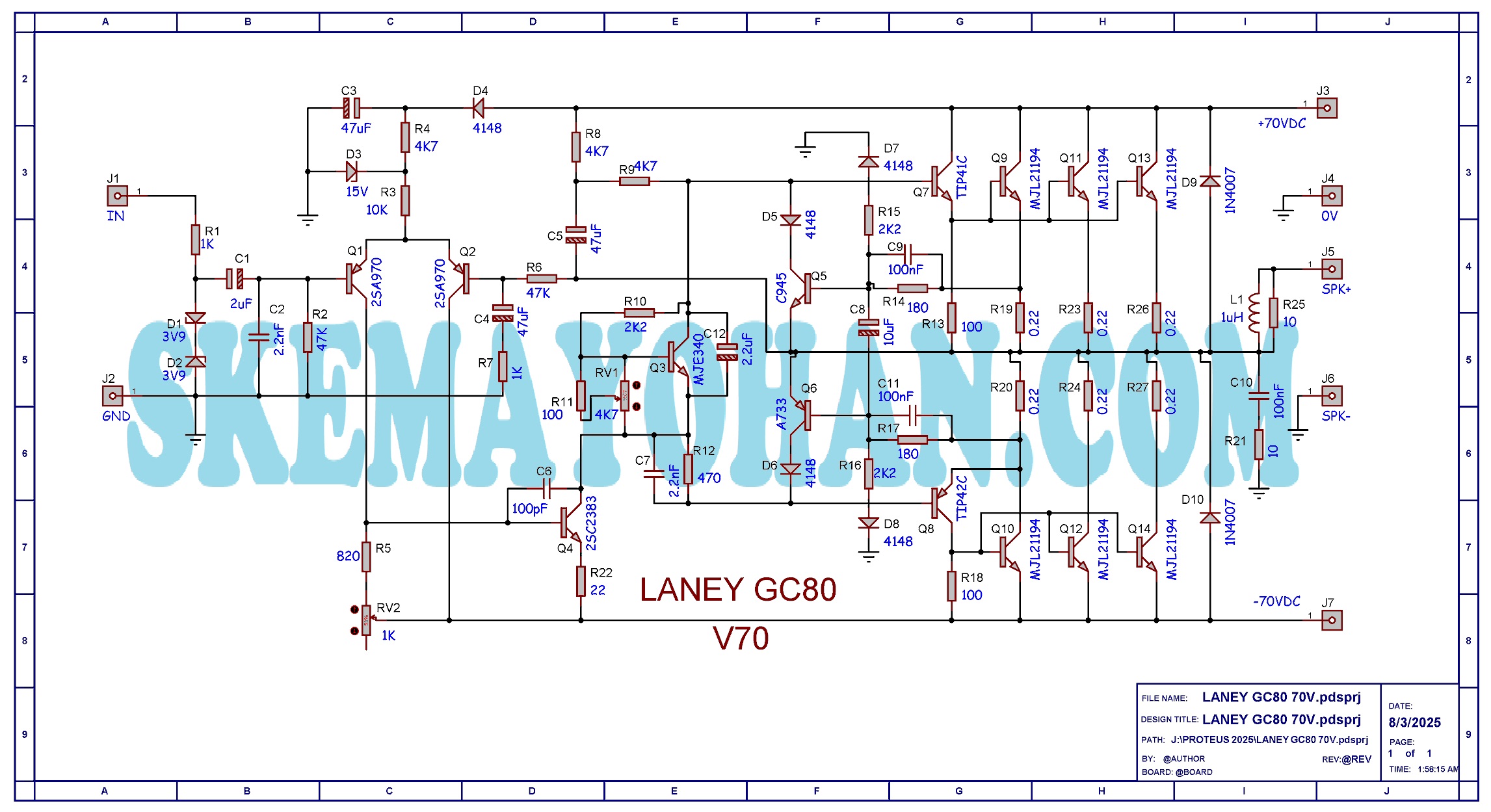
Kloning Power Quasi LAney delapan buah 2SC disini adalah sebuah kloning Power dari produk ampli LANEY seri GC80 namun telah naik daya dan ada tambahan fitur.
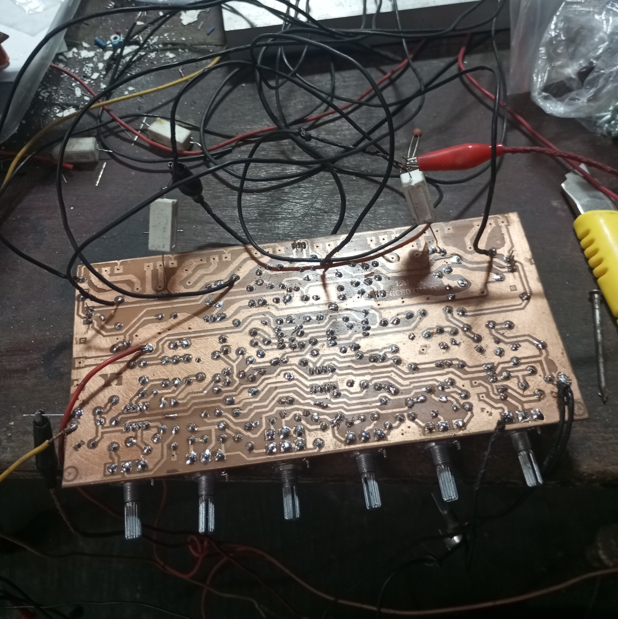
Kloningan kali ini adalah membikin PCb Protoype nya dan memasang komponen sesuai dengan petunjuk.
Tulisan tentang GC80 pernah saya tulis di YOHAN FROM INDONESIA pada 14 september 2024 lalu dan kali ini saya modifikasi kembali karena ada beberapa komponen yang tidak sesuai dengan selera saya.
Table of Contents
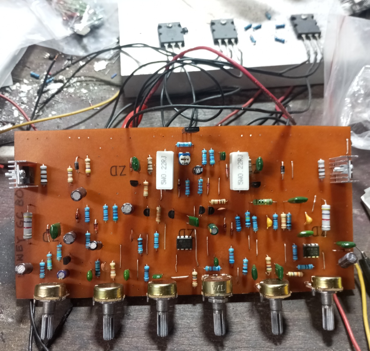
HASIL PROTOTYPE
Berikut ini adalah tampilan protoype LANEY GC80 yang telah ada fitur Subwoofer dan Tone Control berfitur Middle Sweep nya.
PENGGANTIAN TRANSISTOR YANG SULIT DIPEROLEH
Untuk informasi, saya terpaksa mengganti transistor pendukung rangkaian ini karena kesulitan memperleh nomer transistor ini.
Akhirnya saya menganti nomer transistor menjadi berikut:
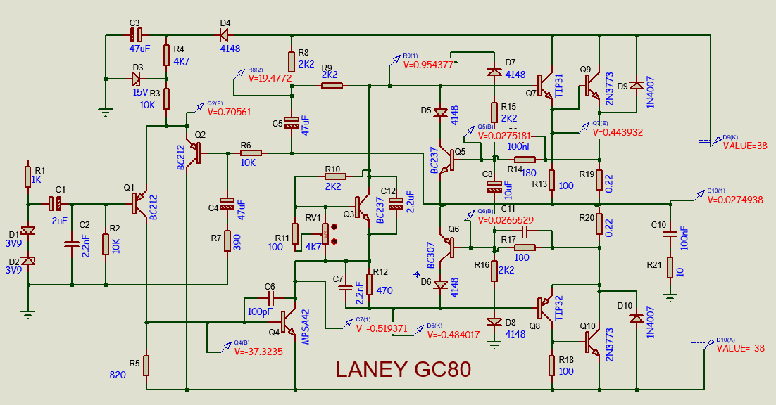
- BC212 ganti dengan 2N5401,
- MPSA42 ganti dengan 2N5551,
- BC237 ganti dengan 2N5551,
- BC307AP ganti dengan 2N5401,
- TIP31 ganti dengan 2SC2073,
- TIP32 ganti dengan 2SA940.
Setelah transistor ini terpasang maka kita bisa melakukan tes modul ini.
HASIL TES MEJA
Tidak semua transistor Final saya pasang. Saya hanya pasang 1 set transitor yang ada komponen pengumpan OCP ( Over Curernt Protection ) saja.
Jika tes ini berhasil maka semua transistor akan kita pasang dan tegangan Supply kita naikkan ke angka yang lebih tinggi.
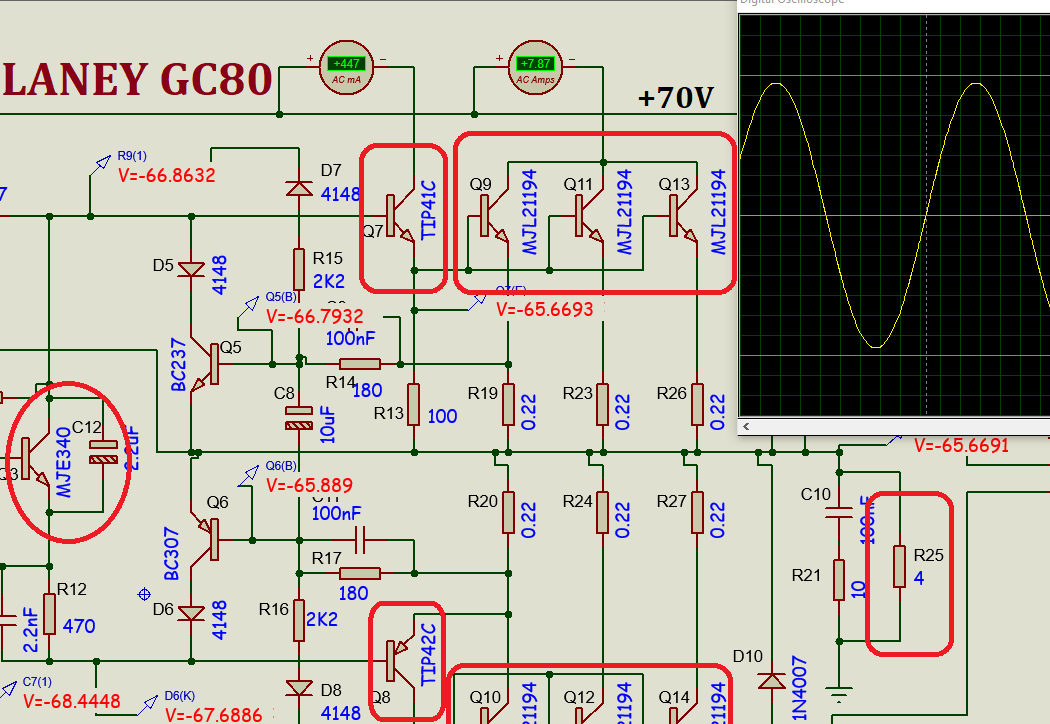
Pada modul ini menggunakan tegangan supply mulai dari 55VDC hingga 75VDC. Untuk membikin rangkaian ini optimal maka kita bikin 65VDC simetris.
Pada tes pertama ini menggunakan tegangan supply 35VDC simetris untuk bermain aman dan pencegahan kerusakan komponen transistor Final.
TEGANGAN OUTPUT MENDEKATI 0,00VDC
Ketika modul ini saya tes dengan tegangan 35VDC, Output terminal ke speaker terukur -0,06VDC. Ini masih aman. Namun ini harus kita sesuaikan untuk mendekati 0 mV.
TRANSISTOR VAS KEPANASAN
Pada tegangan tes 35VDC, transistor VAS mengalami kepanasan. Transistor yang terpasang adalah 2N5551 yang memiliki dissipasi daya 625mW menurut DATASHEETS.
Ketika saya pasang paralel transistor ini, panas transistor menghilang.
Ini berarti memerlukan dissipasi daya lebih dari 600mW pada transistor VAS.
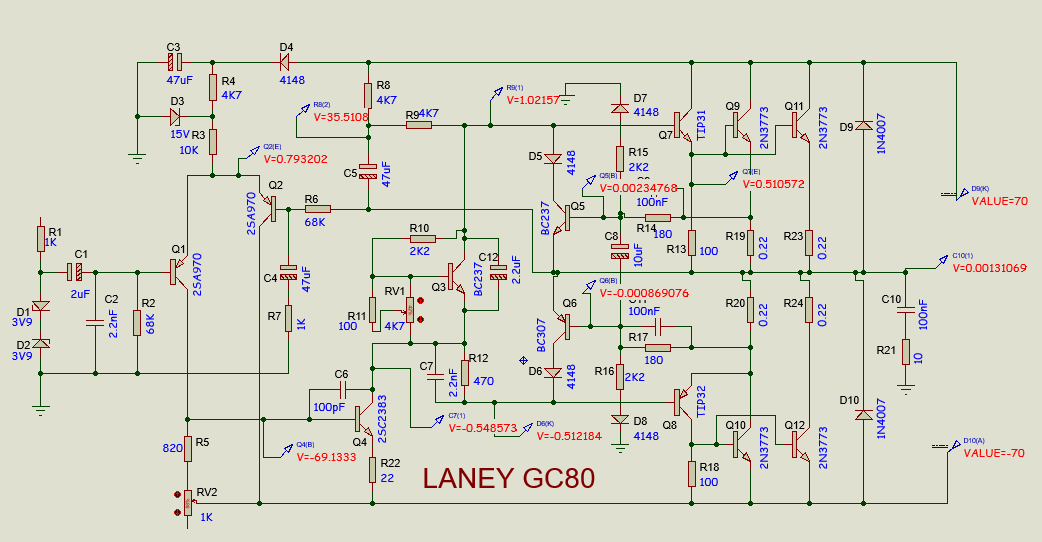
MODIFIKASI ULANG KLONING POWER QUASI LANEY
Beberapa komponen yang terpaksa saya ubah adalah sama dengan yang telah saya jelaskan di atas, yaitu perubahan nomer transistor:
BC212, MPSA42, BC237, BC307AP, TIP31, dan TIP32.
Sedangkan komponen lainnya yang harus kita ubah adalah:
Potensio MID, arah putaran ternyata terbalik,
Komponen penentu freq middle diubah,
Sehingga skema berubah “SEDIKIT” menjadi seperti berikut:

PERUBAHAN LAYOUT
Layout harus saya ubah kembali untuk menyesuaikan komponen transistor yang telah terpasang.
Hasil revisi Layout adalah menjadi seperti ini.
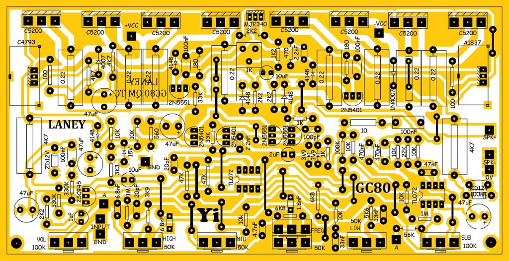
Bandingkan dengan Layout sebelumnya dibawah ini:

Berubah sedikit bukan?
Namun para ahli skema dan ahli PCB pasti paham dimana permbedaan 2 buah Layout PCB ini.
PERAKITAN ULANG KLONING POWER QUASI LANEY
Hasil Layout ini akan saya buatkan PCB kembali untuk pembikinan prototype.
Masih dalam proses.
Nanti apabila berhasil, tinggal mencetakkan prototype ini di tukang PCB terdekat.
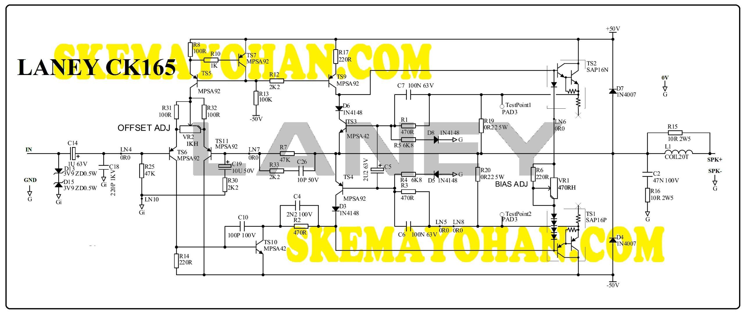
Schematic LANEY lainnya ada di YOHAN FROM INDONESIA.